|
With most electronic hardware moving towards reduced plans, printed circuit boards inside them should hold a significant number of parts per unit square region. With parts pressed so near one another, plans are normally on the limits and manufacturers should follow tight PCB creation resilience. One more element of these plans is the utilization of parts with extremely high pin count, prompting exceptionally fine pitch between the pins. This is the beginning of the name fine-pitch PCB assembly, another name being high-thickness PCB assembly. At Acme Circuits, we plan and gather fine-pitch PCBs. According to our experience, adhering to a couple of straightforward nonexclusive guidelines can fundamentally expand the possibilities of an effective assembly of fine-pitch circuit boards:
Planning fine-pitch circuit boards As expressed before, fine-pitch circuit boards frequently contain some fine-pitch parts. Planning such boards calls for incredible consideration and contemplations from the creator, as they should lay tracks extremely near one another, yet additionally precisely space them between minuscule cushions and vias. 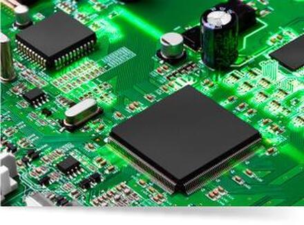 The expense of such boards goes up as the little cushions require extremely high accuracy from the pick and spot machines-much more so when the parts are without leads and of the framework exhibit type. The assembly interaction might require X-beam review strategies.
The planner should likewise keep up with cozy associations with the board fabricator, as the plan of fine-pitch boards can undoubtedly break the capacities of numerous nonexclusive merchants. We ensure our abilities and hardware can undoubtedly meet the subtleties and choices of the fine-pitch board originator. We additionally give our clients basic rules on the dangers connected with the plan and creation of fine-pitch PCB plan and assembly. We have encountered engineers and our help cooperation with our clients to direct them in guaranteeing they get the most noteworthy conceivable nature of fine-pitch PCB assembly manufacturing and exporting. Challenges in fine-pitch PCB layout Whenever there are various parts inside the restricted space of a board, the architect can confront significant design difficulties. This typically brings about the originator making various preliminaries for accomplishing the ideal design. The planner commonly starts the format by bringing in unplaced parts from a schematic. The test starts with populating the board while setting the parts as near one another as could be expected. They should likewise permit satisfactory dispersing for presenting follows in the middle and adding power planes. While follows convey signals, power planes convey voltage and current starting with one part then onto the next. The test can likewise incorporate circuitry working at different velocities. For example, the board might contain simple circuits working at low frequencies, computerized circuitry working at medium and high velocities, and tracks conveying high power. The test is in setting them minimally, while not permitting them to impede each other. For this to be an effective plan, the accompanying advances are vital. Choice of proper components To accomplish the most minimal design, it is important to choose suitable parts that while meeting the practical prerequisites are likewise sufficiently minuscule to save board space. Typically, this is a split the difference between investment funds presented by the part ready space and the expense investment funds the part offers. Albeit a little part saves board space, it costs really during the assembly. Populating fine-pitch parts requires more exactness, and requests explicit sorts of investigation. For example, ball matrix cluster or BGA parts are extremely minimized yet require more prominent precision while setting them, and X-beam review subsequent to binding. By and large, cost increments as resistances get tighter. Thusly, board fashioners should offset cost of assembly with part size. Assuming the need is plan smallness, the originator can utilize the littlest parts accessible. Most IC manufacturers understand this compromise and proposition similar part in different bundles. The planner can choose the fitting bundle by looking into datasheets. The planner should likewise keep a harmony between the part size and rating while at the same time planning for high densities. This is pertinent something else for uninvolved parts like resistors and capacitors that are driven by power appraisals. The fashioner should likewise be cautious in presenting underestimated parts in the plan, as these can welcome on outlandish dangers. Characterizing the board size When the fashioner has characterized the schematic and indicated every one of the parts, they should characterize a sensible size of the board. Normally there can be mechanical imperatives, with an actual cut-off to the X, Y, and Z aspects. The originator should utilize these requirements from the beginning. Notwithstanding, on the off chance that the requirements are as yet being worked on, the architect has a room to change the size of the board. The fashioner should initially check the littlest size the board might perhaps accomplish. The most ideal way to do this is to put every one of the huge parts like connectors on the external fringe. Then, at that point, they should put the biggest ICs, saving assessed space for any breakout signals. They should likewise save space for delicate follows, and sort out for disconnecting them from the remainder of the board. Examining with the board producer can prompt picking standard or preset board sizes, which might cut down creation costs. Now and then utilizing 3D models for the board and cumbersome parts can assist with characterizing the size and state of the board prior to settling. In the wake of settling on the size of the board, the architect can begin with the design and steering. A conversation with the merchant of the board is fundamental at this stage to settle on the legitimate plan rules, as they should line up with the PCB creation abilities of the seller. Significant contemplations incorporate through sizes, clearances and dividing, and follow width. At this stage, planners can consider compromises for cost decrease. Acme Circuits offers numerous choices that our clients can use to adjust capacities against cost. By laying out the fitting plan rules at this stage, our clients can meet their end-cost targets. Part placement When the creator has cleared the plan rules and abilities with the merchant, they can begin the part situation on the board. This is for the most part a work in view of preliminary as the parts should be pressed near one another, yet with satisfactory room for visa, follows, planes from there, the sky is the limit. Acme Circuits suggests beginning with the arrangement and directing of high velocity parts first, trailed by those utilizing high power. With mechanical parts and connector put at the fringe of the board, the originator has laid out an essential system from where they can continue further. Extra considerations For enhancing space in fine-pitch plan, architects frequently consider extra factors, for example,
Conclusion PCB creation and assembly is dependably a harmony among intricacy and cost contemplations. This applies for fine-pitch PCB assembly designs too. Acme Circuits can offer a few compromises that save our clients significant measures of cash and time while creating and delivering their fine-pitch PCBs.
0 Comments
Leave a Reply. |
