|
With better than ever advances, the field of Printed circuit board assembly (PCBA) has been continually developing. The gadgets business is driven by developments and better assembling strategies that are filling in ubiquity. Further developed advances additionally request the producers to focus on the expense factors too. In such a situation, they need to track down ways of exploiting the current market patterns while adjusting costs and consolidating new subject matters. With the current innovations getting outdated, producers must stay aware of the most recent patterns and improvements. Allow us to help you through the absolute most significant improvements in the PCB assembly industry, in the new times. PCB Manufacturing Trends and Their Impact The PCB producing industry has seen a few significant formative changes. Underneath given are the absolute greatest PCBA manufacturing patterns in the new times. Rising interest for brilliant and more modest gadgets: With expanding interest for shrewd gadgets, hardware makers are expected to team up with innovation accomplices to construct and support the network expected by such gadgets. The gadgets are getting more modest and more intricate. In this manner, PCB sheets likewise must be more slender so they can fit in the savvy gadgets. Here, the producers must be adaptable to fuse such changes effectively and rapidly. Rising idea of 'Practice environmental awareness': Environmental worries top the rundown of issues that need prompt consideration. Hence, producers face the steady interest to embrace climate agreeable assembling processes. The rising attention to stick to the RoHS compliances has added to the rising interest for sans lead items that safeguards clients, as well as limits the carbon impression of the hardware producer. Creation of halogen and without lead PCBs is developing quickly and producers need to set sure they live up to the developing assumptions. 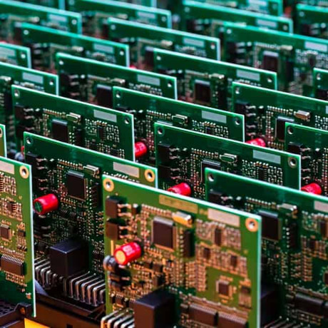
Quality is the key: With the developing notoriety of PCB testing and inspection techniques, it is becoming vital to keep up with the nature of the items. Progressed quality testing components have made it critical to guarantee that the nature of the PCB is kept up with all through the whole assembling process. 3D mix and inserted parts: 3D combination is one of the most potential PCB configuration drifts that request more modest and denser sheets. This is satisfied by arrangement of implanted parts, which work with expanded intricacy, decreased assembling costs and further developed framework execution. Development in the clinical gadget innovation market: The field of medication is perhaps the greatest adopter of mechanical headways. The decrease in the size of the PCBs and their expanded intricacy will help clinical workplaces, research labs and assembling plants. This is on the grounds that they all utilization little PCB driven machines. These machines are intended to further develop exactness and efficiency. In the past post, different famous PCB assessment procedures were examined. PCB testing is the following period of the PCBA manufacturing, after PCB assessment. When the PCB goes through investigation, it is viewed as prepared for testing. There are different trying techniques utilized by PCB makers to examine the functioning state of parts. What are they? The post talks about these strategies exhaustively. Different PCB Testing Methods Employed by PCB Manufacturers There are a few strategies being used today, which permit PCB producers to test the legitimacy of parts and the PCB. Coming up next are a few demonstrated and tried techniques utilized by PCBA manufacturers in India & world. In-circuit Testing: Also alluded to as ICT, this testing basically performed to really look at the part arrangement. An electric test is utilized over a populated printed circuit board to check factors like opens and shorts, capacitance, opposition, and so on In-circuit testing includes a few individual tests, which are directed on parts. The board is viewed as great, assuming it clears this multitude of individual tests. Practical Testing: This is a last advance in the PCB fabricating. Practical testing re-enacts the genuine climate wherein the PCB is relied upon to perform. Hot Mock Up testing is one of the most well-known types of practical testing, which is directed to break down the working of the PCB. This testing is frequently utilized in blend with flying test testing and ICT to guarantee the PCBA is sans mistake and vigorous. Limit Scan Testing: This testing is performed for testing wire lines on a populated printed circuit board. It is additionally used to investigate pin states in coordinated circuits, as well as to quantify and examine its shocks. Flying Probe Testing: It is likewise alluded to as Fixtureless in-circuit testing (FICT), and is utilized for recognizing openness issues. This testing is great for testing models, and mid-volume types. This testing is generally led utilizing a bed-of-nails apparatus, which can be effectively altered based on the PCBA plan. Tin Whisker Testing: Tin is the well-known completing material utilized by PCB makers. This material develops into stubbles, which might direct power, and influence the activity of the application. Normally, these hairs are revised utilizing conformal covering, or tin completing is supplanted with metal. Optical Microscopy Testing: This testing technique is utilized for recognizing deserts, issues, as well as a few different issues in PCB assembly. Optical Microscopy Testing is directed utilizing a powerful magnifying instrument. Every part is isolated into a few miniature areas and tried under the magnifying instrument. This procedure is frequently joined with miniature separating to guarantee the substantial exhibition of the example. Metallographic Preparation: The technique is otherwise called cross-separating or miniature segment examination. The cross segment is led to explore parts, shorts, or opens, thermo-mechanical disappointments, and so on during testing, the bind joint internals are investigated. A 2D area is taken out from the PCB, and set in an epoxy pitch. At the point when it sets, the part is retreated and uncovered. Abrasives are utilized for subsiding. The uncovered part is contrasted and other non-broken parts, and is inspected utilizing an electron/optical microscopy. Consume in Testing: The testing helps PCB assembly benefits approve the presentation of PCB, in actuality, conditions. PCB Contamination Testing: Although PCB assembling and assembly happens in the controlled climate, still the possibilities of tainting is high from different recognized and non-distinguished sources. Motion deposits, ill-advised treatment of PCBs, and a response of synthetic substances are a couple of normal wellsprings of pollution. During the cycle, a PCB is inundated in an answer and left for a specific time frame period. The constitution of the dissolvable changes because of the presence of ionic toxins. Each of the previously mentioned PCB testing processes have run of the mill benefits. You can contact the producer to comprehend different advantages of the testing system. Acme Circuits is one of the notable PCB assembly specialist organizations in the US. The organization utilizes different PCB examination and testing administrations talked about in the posts.
0 Comments
Leave a Reply. |
